loading...

مطالب تخصصی و فوق تخصصی (برق _الکترونیک) و (دکترای نانو _ میکرو الکترونیک)

توضیحی کامل درباره مباحث تخصصی و فوق تخصصی برق_الکترونیک و دکترای نانو _ میکرو الکترونیک

بازدید : 4
دوشنبه 10 فروردين 1404 زمان : 10:01
  • 1
  • 2
  • 3
  • 4
  • 5

مطالب تخصصی و فوق تخصصی (برق _الکترونیک)  و (دکترای نانو _ میکرو الکترونیک)

_ Nanoplasmonics and Nanoelectronics Model Section

Nanoelectronics and (nanoplasmonics) application of nanoelectromagnetic waves in nanometer specifications in two-dimensional, one-dimensional and even zero-dimensional structures

Researcher and Author: Dr. ( Afshin Rashid)

مطالب تخصصی و فوق تخصصی (برق _الکترونیک)  و (دکترای نانو _ میکرو الکترونیک)

Note: In the structure that constitutes nanostructures (nanoplasmonics), the created volume of the electromagnetic field is locally compressed and enhanced. Small changes in the dielectric surrounding the nanovolume affect the resonance of surface plasmons, so that these changes are reflected in the amount of scattered radiation, absorbed radiation, or a change in its wavelength.

Nanostructure is defined as any structure with one or more dimensions and is measured in the nanometer range. Nanostructures refer to materials or structures that have at least one dimension between 1 and 100 nanometers . The importance of the nanoscale is in changing the properties and characteristics of materials in these dimensions. Properties such as electrical conductivity, electromagnetic properties, etc. The beginning of changing the properties of materials by miniaturizing them depends more than anything on the type of material and the desired property. For example, as the dimensions of a material are reduced, generally some of the electromagnetic properties of nanomolecular materials such as the conductivity of nanoparticle particles in the material improve. This increase in strength does not only occur in the range of a few nanometers, and the strength of a material of several tens or even hundreds of nanometers may be much greater than that of a large-scale bulk material. These changes can be measured using optical characteristics. The oscillation of surface electrons and the electric field around them shows in the resonance of localized surface plasmons.

مطالب تخصصی و فوق تخصصی (برق _الکترونیک)  و (دکترای نانو _ میکرو الکترونیک)

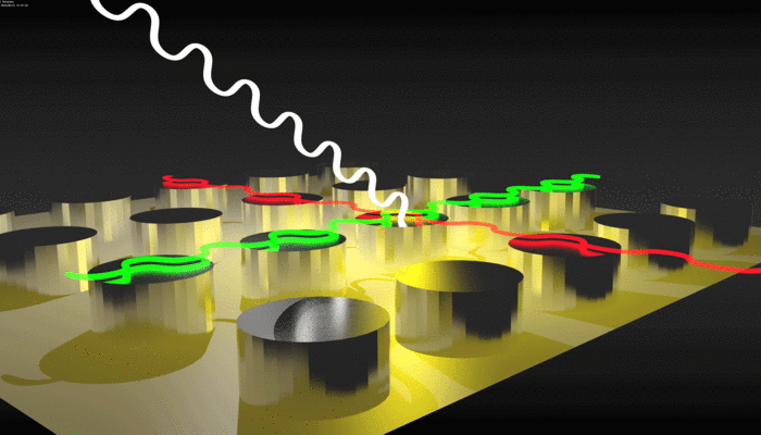
For example, as the dimensions of a nanostructured material (nanoplasmonics) decrease , some of the mechanical properties of the material, such as strength, generally improve. This increase in strength does not occur only in the range of a few nanometers, and the strength of a material of several tens or even hundreds of nanometers may be much greater than that of a large-scale bulk material. On the other hand, changes in some properties, such as color and magnetic properties, may occur in dimensions of only a few nanometers. Nanoplasmonics is expressed based on the interaction process between electromagnetic waves and conduction electrons in metals with nanoscale dimensions . Analytically, the reason for the rapid drop in energy of electrons passing through metals is that this energy is spent on the collective and oscillatory motion of free electrons in the metal, which is called a plasmon. These nanostructures consist of metal and dielectric, whose dimensions are below the excitation wavelength (the wavelength of the radiation that excites plasmonic waves).

مطالب تخصصی و فوق تخصصی (برق _الکترونیک)  و (دکترای نانو _ میکرو الکترونیک)

Conclusion:

In the nanostructures (nanoplasmonics), the created volume of the electromagnetic field is locally compressed and enhanced. Small changes in the dielectric surrounding the nanovolume affect the resonance of surface plasmons, so that these changes are manifested in the amount of scattered radiation, absorbed radiation or a change in its wavelength.

Researcher and Author: Dr. ( Afshin Rashid)

Specialized PhD in Nano-Microelectronics

بازدید : 13
شنبه 8 فروردين 1404 زمان : 11:11
  • 1
  • 2
  • 3
  • 4
  • 5

مطالب تخصصی و فوق تخصصی (برق _الکترونیک)  و (دکترای نانو _ میکرو الکترونیک)

_ Nanoplasmonics and Nanoelectronics Model Section

Nanoelectronics and plasmonics model for manufacturing and producing nanoelectrical systems (dimensions 1 to 100 nanometers)

Researcher and Author: Dr. ( Afshin Rashid)

مطالب تخصصی و فوق تخصصی (برق _الکترونیک)  و (دکترای نانو _ میکرو الکترونیک)

مطالب تخصصی و فوق تخصصی (برق _الکترونیک)  و (دکترای نانو _ میکرو الکترونیک)

Note: Nano Systems are composed of various organic or inorganic materials whose capabilities and characteristics, such as their size, range from 1 to 100 nanometers. Nano particles are the main components of Nano Systems.

The first broad description of nanotechnology refers to the specific goal of the technology of precisely manipulating atoms and molecules to make products on a large scale, also known as a nanosystem .

مطالب تخصصی و فوق تخصصی (برق _الکترونیک)  و (دکترای نانو _ میکرو الکترونیک)

Nanosystems are molecular-scale functions. This includes both current work and more advanced concepts. In its original sense, nanotechnology refers to the envisioned ability to build things from the bottom up, using techniques and tools that are developed to produce complete, high-performance products. Nanosystems introduced the idea of ​​nanoscale "assembly" that can make copies of itself and of itself. Among other things, arbitrary complexity with atomic control is very widespread and applicable in Nanosystems. Nanocomputers and nanoassemblers are also sub-groups of Nanosystems. Nanoparticles are the main components of all Nanosystems. Nanotechnology can be used to produce nanoparticle particles by changing the properties of atoms. When materials are studied at the nanoscale, the reactions and behavior of atoms are completely different compared to when they are studied at the molecular level, because in this realm the physical properties of the materials change. This is like dropping a ball into a container and taking another ball out of that container. The difference in the nano realm is so great that even the color, melting point, chemical properties, etc. of the materials outside this range are completely different. With the technological approach towards the accumulation of optoelectronic circuits, the fabrication problems and phenomena that helped prevent further compaction of the structure led to the use of plasmonic structures and plasmonic waves. These nanostructures consist of metal and dielectric whose dimensions are below the excitation wavelength (the wavelength of the radiation that excites the plasmonic waves).

مطالب تخصصی و فوق تخصصی (برق _الکترونیک)  و (دکترای نانو _ میکرو الکترونیک)

Conclusion:

Nano Systems are composed of various organic or inorganic materials whose capabilities and characteristics, such as their size, range from 1 to 100 nanometers. Nano particles are the main components of Nano Systems.

Researcher and Author: Dr. ( Afshin Rashid)

Specialized PhD in Nano-Microelectronics

تعداد صفحات : -1

آمار سایت
  • کل مطالب : 0
  • کل نظرات : 0
  • افراد آنلاین : 4
  • تعداد اعضا : 0
  • بازدید امروز : 64
  • بازدید کننده امروز : 30
  • باردید دیروز : 28
  • بازدید کننده دیروز : 28
  • گوگل امروز : 0
  • گوگل دیروز : 0
  • بازدید هفته : 611
  • بازدید ماه : 1399
  • بازدید سال : 2797
  • بازدید کلی : 2862
  • کدهای اختصاصی